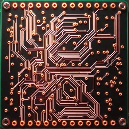
Photo Potting
At CADDINE SYSTEMS PVT LTD , we offer high-precision film plotting services for PCB manufacturing, ensuring accurate and reliable image transfer for your circuit designs. Using advanced photo plotters , we convert your Gerber or PDF files into high-resolution photographic films with precise line widths and clear details ready for the PCB image transfer process.Our film plotting process is designed for accuracy, consistency, and high-quality imaging:
1.Data Input
We accept design data in Gerber or PDF format.
Files are carefully checked for accuracy and layer alignment before plotting.
2.Photo Plotting (Imaging)
The design image is transferred onto a 4 mil or 5 mil thickness film using a photo plotter.
The plotter exposes the film using controlled light exposure , creating a precise image of the PCB pattern.
3.Developing Process
The exposed film is then developed automatically using a dedicated developing machine.
The machine performs developing, rinsing, and drying all in one continuous, controlled process ensuring clarity and high contrast in the final film.
4. Quality Check
Each plotted film is inspected for line width accuracy, registration, and resolution before delivery.
Technical Capabilities
Film Thickness: 4 mil / 5 mil
Accepted Formats: Gerber, PDF
Plotting Resolution: Up to 25,000 dpi
Alignment Accuracy: ±10 microns
Maximum Film Size: 12” x 24”]
Partner with Us for precise and reliable Film plotting services that support your PCB manufacturing.